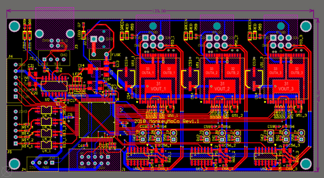
Printed Circuit Board Layout

ETConcept offer expertise in PCB layout design, from small-footprint, power-optimized solutions to high-end, rugged systems built around various embedded systems. We also isolate critical signals and nets to prevent crosstalk and system noise.

We work with the best tools

Altium Designer Software allows us to easily develop our PCB layout designs, integrating it into the design process, allowing future project modifications.

Our PCB layout expertise include

  • Footprint design

  • Board outline

  • Layout rules and constraints

  • Component placement

  • PCB stackup design

  • IDF and DXF mechanical review

  • Routing

  • Power splits

  • Test points

  • Silk screen

  • Gerber file generation​

We work with the following technology

  • RF routing techniques and isolation

  • Differential pairs

  • Controlled impedance

  • Low-cost PCB material FR4

  • Rigid flex PCB

  • Stacked and microvias